Due to their role in the fabrication of electronic devices, semiconductors are an important part of our lives. Imagine life without electronic devices. There would be no radios, no TV’s, no computers, no video games, and poor medical diagnostic equipment. Although many electronic devices could be made using vacuum tube technology, the developments in semiconductor technology during the past 50 years have made electronic devices smaller, faster, and more reliable. Think for a minute of all the encounters you have with electronic devices. How many of the following have you seen or used in the last twenty-four hours? Each has important components that have been manufactured with electronic materials.
“A semiconductor is a material that is between conductors and insulators in its ability to conduct electrical current. A semiconductor in its pure (intrinsic) state is neither a good conductor nor a good insulator. Single-element semiconductors are antimony (Sb), arsenic (As), astatine (At), boron (B), polonium (Po), tellurium (Te), silicon (Si), and germanium (Ge). Compound semiconductors such as gallium arsenide, indium phosphide, gallium nitride, silicon carbide, and silicon germanium are also commonly used. The single-element semiconductors are characterized by atoms with four valence electrons. Silicon is the most commonly used semiconductor”.
On the other hand Semiconductors materials such as silicon (Si), germanium (Ge) and gallium arsenide (GaAs), have electrical properties somewhere in the middle, between those of a “conductor” and an “insulator”. They are not good conductors or good insulators (hence their name “semi”-conductors). They have very few “free electrons” because their atoms are closely grouped together in a crystalline pattern called a “crystal lattice” but electrons are still able to flow, but only under special conditions.
The ability of semiconductors to conduct electricity can be greatly improved by replacing or adding certain donor or acceptor atoms to this crystalline structure thereby, producing more free electrons than holes or vice versa. That is by adding a small percentage of another element to the base material, either silicon or germanium.
On their own Silicon and Germanium are classed as intrinsic semiconductors, that is they are chemically pure, containing nothing but semi-conductive material. But by controlling the amount of impurities added to this intrinsic semiconductor material it is possible to control its conductivity. Various impurities called donors or acceptors can be added to this intrinsic material to produce free electrons or holes respectively.
This process of adding donor or acceptor atoms to semiconductor atoms (the order of 1 impurity atom per 10 million (or more) atoms of the semiconductor) is called Doping. The as the doped silicon is no longer pure, these donor and acceptor atoms are collectively referred to as “impurities”, and by doping these silicon material with a sufficient number of impurities, we can turn it into an N-type or P-type semi-conductor material.
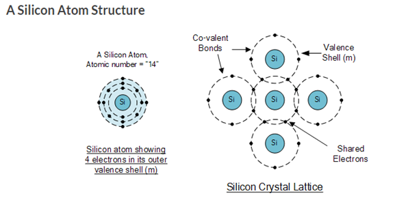
The most commonly used semiconductor basics material by far is silicon. Silicon has four valence electrons in its outermost shell which it shares with its neighboring silicon atoms to form full orbitals of eight electrons. The structure of the bond between the two silicon atoms is such that each atom shares one electron with its neighbor making the bond very stable.
As there are very few free electrons available to move around the silicon crystal, crystals of pure silicon (or germanium) are therefore good insulators, or at the very least very high value resistors.
Silicon atoms are arranged in a definite symmetrical pattern making them a crystalline solid structure. A crystal of pure silica (silicon dioxide or glass) is generally said to be an intrinsic crystal (it has no impurities) and therefore has no free electrons.
But simply connecting a silicon crystal to a battery supply is not enough to extract an electric current from it. To do that we need to create a “positive” and a “negative” pole within the silicon allowing electrons and therefore electric current to flow out of the silicon. These poles are created by doping the silicon with certain impurities.
The diagram below structure and lattice of a ‘normal’ pure crystal of Silicon.
N-type Semiconductor Basics
In order for our silicon crystal to conduct electricity, we need to introduce an impurity atom such as Arsenic, Antimony or Phosphorus into the crystalline structure making it extrinsic (impurities are added). These atoms have five outer electrons in their outermost orbital to share with neighboring atoms and are commonly called “Pentavalent” impurities.
This allows four out of the five orbital electrons to bond with its neighboring silicon atoms leaving one “free electron” to become mobile when an electrical voltage is applied (electron flow). As each impurity atom “donates” one electron, pentavalent atoms are generally known as “donors”.
Antimony (symbol Sb) as well as Phosphorus (symbol P), are frequently used as a pentavalent additive to silicon. Antimony has 51 electrons arranged in five shells around its nucleus with the outermost orbital having five electrons. The resulting semiconductor basics material has an excess of current-carrying electrons, each with a negative charge, and is therefore referred to as an N-type material with the electrons called “Majority Carriers” while the resulting holes are called “Minority Carriers”.
When stimulated by an external power source, the electrons freed from the silicon atoms by this stimulation are quickly replaced by the free electrons available from the doped Antimony atoms. But this action still leaves an extra electron (the freed electron) floating around the doped crystal making it negatively charged.
Then a semiconductor material is classed as N-type when its donor density is greater than its acceptor density, in other words, it has more electrons than holes thereby creating a negative pole as shown.
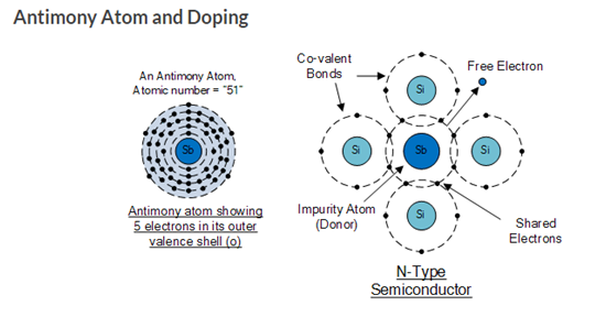
The diagram above shows the structure and lattice of the donor impurity atom Antimony.
P-Type Semiconductor Basics
If we go the other way, and introduce a “Trivalent” (3-electron) impurity into the crystalline structure, such as Aluminum, Boron or Indium, which have only three valence electrons available in their outermost orbital, the fourth closed bond cannot be formed. Therefore, a complete connection is not possible, giving the semiconductor material an abundance of positively charged carriers known as holes in the structure of the crystal where electrons are effectively missing.
As there is now a hole in the silicon crystal, a neighboring electron is attracted to it and will try to move into the hole to fill it. However, the electron filling the hole leaves another hole behind it as it moves. This in turn attracts another electron which in turn creates another hole behind it, and so forth giving the appearance that the holes are moving as a positive charge through the crystal structure (conventional current flow).This movement of holes results in a shortage of electrons in the silicon turning the entire doped crystal into a positive pole. As each impurity atom generates a hole, trivalent impurities are generally known as “Acceptors” as they are continually “accepting” extra or free electrons.
Boron (symbol B) is commonly used as a trivalent additive as it has only five electrons arranged in three shells around its nucleus with the outermost orbital having only three electrons. The doping of Boron atoms causes conduction to consist mainly of positive charge carriers resulting in a P-type material with the positive holes being called “Majority Carriers” while the free electrons are called “Minority Carriers”.
Then a semiconductor basics material is classed as P-type when its acceptor density is greater than its donor density. Therefore, a P-type semiconductor has more holes than electrons.

The diagram above shows the structure and lattice of the acceptor impurity atom Boron.
Majority and Minority Carriers Since most of the current carriers are electrons, silicon (or germanium) doped with pentavalent atoms is an n-type semiconductor (the n stands for the negative charge on an electron). The electrons are called the majority carriers in n-type material. Although the majority of current carriers in n-type material are electrons, there are also a few holes that are created when electron-hole pairs are thermally generated. These holes are not produced by the addition of the pentavalent impurity atoms. Holes in an n-type material are called minority carriers.
Semiconductor Basics Summary
N-type (e.g. doped with Antimony)
These are materials which have Pentavalent impurity atoms (Donors) added and conduct by “electron” movement and are therefore called, N-type Semiconductors.
In N-type semiconductors there are:
- The Donors are positively charged.
- There are a large number of free electrons.
- A small number of holes in relation to the number of free electrons.
- Doping gives:
- Positively charged donors.
- Negatively charged free electrons.
- Supply of energy gives:
- Negatively charged free electrons.
- Positively charged holes.
P-type (e.g. doped with Boron)
These are materials which have Trivalent impurity atoms (Acceptors) added and conduct by “hole” movement and are therefore called, P-type Semiconductors.
In these types of materials are:
- The Acceptors are negatively charged.
- There are a large number of holes.
- A small number of free electrons in relation to the number of holes.
- Doping gives:
- Negatively charged acceptors.
- Positively charged holes.
- Supply of energy gives:
- Positively charged holes.
- Negatively charged free electrons.
And both P and N-types as a whole are electrically neutral on their own.
Antimony (Sb) and Boron (B) are two of the most commonly used doping agents as they are more freely available compared to other types of materials. They are also classed as “metalloids”. However, the periodic table groups together a number of other different chemical elements all with either three, or five electrons in their outermost orbital shell making them suitable as a doping material.
These other chemical elements can also be used as doping agents to a base material of either Silicon (Si) or Germanium (Ge) to produce different types of basic semiconductor materials for use in electronic semiconductor components, microprocessor and solar cell applications. These additional semiconductor materials are given below.
