Although the crystal semiconductor diode was popular before the thermionic diode (also known as vacuum tubes, tubes, or valves), thermionic and solid state diodes were developed in parallel.
The basic principle of operation of thermionic diodes was discovered by Frederick Guthrie in 1873. Guthrie discovered that a positively-charged electroscope could be discharged by bringing a grounded piece of white-hot metal close to it (but not actually touching it). The same did not apply to a negatively charged electroscope, indicating that the current flow was only possible in one direction.
The principle was independently rediscovered by Thomas Edison on February 13, 1880. At the time Edison was carrying out research into why the filaments of his carbon-filament light bulbs nearly always burned out at the positive-connected end. He had a special bulb made with a metal plate sealed into the glass envelope, and he was able to confirm that an invisible current could be drawn from the glowing filament through the vacuum to the metal plate, but only when the plate was connected to the positive supply.
Edison devised a circuit where his modified light bulb more or less replaced the resistor in a DC voltmeter and on this basis was awarded a patent for it in 1883. There was no apparent practical use for such device at the time, and the patent application was most likely simply a precaution in case someone else did find a use for the so-called “Edison Effect”.
About 20 years later, John Ambrose Fleming (scientific adviser to the Marconi Company and former Edison employee) realized that the Edison effect could be used as a precision radio detector. Fleming patented the first true thermionic diode in Britain on November 16, 1904 (followed by U.S. Patent 803,684 in November 1905).
The principle of operation of crystal diodes was discovered in 1874 by the German scientist Karl Ferdinand Braun. Braun patented the crystal rectifier in 1899. Braun’s discovery was further developed by Jagdish Chandra Bose into a useful device for radio detection.
The first actual radio receiver using a crystal diode was built by Greenleaf Whittier Pickard. Pickard received a patent for a silicon crystal detector on November 20, 1906.
Other experimenters tried a variety of minerals and other substances, although by far the most popular was the lead sulfide mineral Galena. Although other substances offered slightly better performance, galena had the advantage of being cheap and easy to obtain, and was used almost exclusively in home-built “crystal sets”, until the advent of inexpensive fixed-germanium diodes in the 1950s.
At the time of their invention, such devices were known as rectifiers. In 1919, William Henry Eccles coined the term diode from the Greek roots dia, meaning “through”, and ode, meaning “path”.
Thermionic and gaseous state (vacuum tube) diodes
Thermionic diodes are thermionic-valve devices (also known as vacuum tubes, tubes, or valves), which are arrangements of electrodes surrounded by a vacuum within a glass envelope. Early examples were fairly similar in appearance to incandescent light bulbs.
In thermionic valve diodes, a current through the heater filament indirectly heats the cathode, another internal electrode treated with a mixture of barium and strontium oxides, which are oxides of alkaline earth metals; these substances are chosen because they have a small work function. (Some valves use direct heating, in which a tungsten filament acts as both heater and cathode.) The heat causes thermionic emission of electrons into the vacuum. In forward operation, a surrounding metal electrode called the anode is positively charged so that it electro statically attracts the emitted electrons. However, electrons are not easily released from the unheated anode surface when the voltage polarity is reversed. Hence, any reverse flow is negligible. For much of the 20th century, thermionic valve diodes were used in analog signal applications, and as rectifiers in many power supplies. Today, valve diodes are only used in niche applications such as rectifiers in electric guitar and high-end audio amplifiers as well as specialized high-voltage equipment.
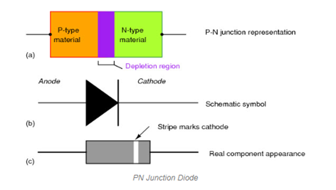
A modern semiconductor diode is made of a crystal of semiconductor like Silicon that has impurities added to it to create a region on one side that contains negative charge carriers (Electrons), called n-type semiconductor, and a region on the other side that contains positive charge carriers (hole), called p-type semiconductor. The diode’s terminals are attached to each of these regions. The boundary within the crystal between these two regions, called PN junction, is where the action of the diode take place. The crystal conducts conventional current in a direction from the p-type side (called the anode) to the n-type side (called the cathode), but not the opposite direction.
Another type of semiconductor diode, the Schottky diode, is formed contact between a metal and a semiconductor rather than by p-n junction.
Current- Voltage (I-V) characteristic:
A semiconductor diode’s behavior in a circuit is given by its current- voltage characteristics or I-V graph (see below diagram). The shape of the curve determined by the transport of charge carriers through the sp-called depletion layer or depletion region that exists at the p-n junction between semiconductors. When a p-n junction is first created, conduction band (mobile electrons from the N-doped region diffuse the P-doped region where there is a large population of holes (vacant place for electrons) with which the electrons “recombines “. When a mobile electron recombines with a hole, both hole and electrons vanish, leaving behind an immobile positively charged donor (dopant) on the N- side and negatively charged acceptor (dopant) on the p-side. The region around the p-n junction becomes depleted of charge carriers and this behaves as an insulator.
However, the width of the depletion region (called the depletion width) cannot grow without limit. For each electrons-hole pair that recombines, a positively-charged dopant ion id the left behind in the N-doped region, and a negatively charged dopant ion is left behind in the P-doped region. As recombination proceeds more ions are created, an increasing electric field develops through the depletion zone which act to slow and then finally stop recombination. At this point, there is a “built-in” potential across the depletion zone.
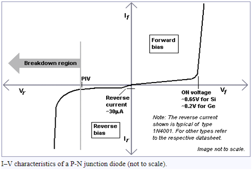
If an external voltage is placed across the diode with the same polarity as the built in potential, the depletion zone continues to act as a insulator, preventing any significant electric current flow (unless electron/hole pairs are actively being created in the junction by, for instance, light. This is the reverse bias phenomenon. However, if the polarity of the external voltage opposes the built-in potential, recombination can once again proceed, resulting in substantial electric current through the p-n junction. (I.e. substantial of electrons and holes recombines at the junction. For silicon diode, the built in potential is approximately 0.6V. This, if an external current passed through the diode, about 0.6V will be developed across the diode such that the P-doped region is positive with respect to the N-doped region and the diode is said to be “turned on” as it has a forward bias.
At very large reverse bias, beyond the peak inverse voltage or PIV, a process called reverse breakdown occurs which causes a large increase in current (i.e. a large numbers of electrons and holes created at, and move away from the p-n junction that usually damage the device permanently. The avalanche diode is deliberately design for use in the avalanche region. In the zener diode, the concept of PIV in no applicable. A zener diode contains a heavily doped p-n junction allowing electrons to tunnel from the valence band of the p-type material to the conduction band of the n-type material, such that the reverse voltage is “ clamped” to known value ( called zener voltage), and avalanche does not occur. Both devices, however, do have a limit to the maximum current and power in the clamped reverse voltage region. Also, following the end of forward conduction in any diode, there is reverse current for a short time. The device does not attain its full blocking capability until the reverse current ceases.
The second region, at reverse biases more positive than the PIV, has only a very small reverse saturation current. In the reverse bias region for a normal P-N rectifier diode, the current through the device is very low in µA rage. However, this is temperature dependent, and at suffiently high temp., a substantial amount of reverse current can be observed in mA or more.
The third region is forward but small bias, where only a small forward current is conducted.
As the potential difference is increased above an arbitrarily defined “cut-in voltage” or “on-voltage” or diode forward voltage drop (Vd)”, the diode current becomes appreciable ( the level of current considered “ appreciable” and the value of cut-in voltage depends on the application), and the diode presents a very low resistance.
The current – voltage curve is exponential. In a normal silicon diode at rated currents, the arbitrary “cut-in” voltage is defined as 0.6 to 0.7 volts.
The value is different for other diode types Schottky diodes can be rated as low as 0.2V and red or blue light-emitting diode (LEDs) can have values of 1.4V and 4.0V respectively.
At higher currents the forward voltage drop of the diode increase. A drop of 1V to 1.5V is typical at full rated current for power diode.
When no voltage is applied across the PN junction diode then the electrons will diffuse to P-side and holes will diffuse to N-side through the junction and they combines. Therefore, the acceptor atom close to the P-type and donor atom near to the N-side id left unutilized. An electrons field is generated by these charge carriers. This opposes further diffusion of charge carriers. Thus, no movement of the region is known as the depletion region or space charge.
Zero biased PN-Junction diode:
In the zero bias junctions, potentially provides higher potential energy to the holes on the P and N side terminals. When the terminals of the junction diode are shorted, few majority charge carriers in the P-side with plenty of energy to overcome the potential barrier to travel across the depletion region.
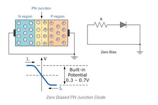
Therefore, with the help of majority charge carriers, the current starts to flow in the diode and it is denoted to as forwarding current. In the same way, minority charge carriers in the N-side move across the depletion region in reverse direction and it is referred to as current.
Potential barrier opposes the movement of electrons and holes across the junction and permit the minority charge carriers to drift across the PN junction. However, the potential barrier helps minority charge carriers in P-type and N-type to drift across the PN-junction, then equilibrium will be established when the majority charge carriers are equal and both moving in reverse direction so that the net result is zero current flowing in the circuit.
This junction is said to be in a state of dynamic equilibrium. When the temperature of the semiconductor is increased, minority charge carriers have been endlessly generated and thus leakage current starts to rise. But, electric current flow since no external source has been connected to the PN-Junction.
Recall Band diagram of Zero biased diode:
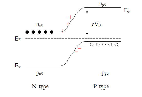
Away from depletion region:
N-side provides supply of free electrons (nn0 large).
P-side provides supply of free holes (pp0 large).
However, due to thermal excitation charge carriers across the junction, we get:
Small Conc.’s np0 of free electrons on P-side.
Small Conc.’s Pn0 of free electrons on N-side.
Potential drop VB across junction ( in zero applied bias):
np0 /nn0 = pn0/pp0 = exp (-eVB/kT) …… [1]
Forward Bias:
When a P-N Junction diode is connected in a forward bias by a positive to the P-type and a negative voltage to the N-type. If the external become more than the value of potential barrier (estimate 0.7V for Si and 0.3V for Ge, the opposition of the potential barriers will be overcome and the flow of current will start because the negative voltage repels electrons near to the junction by giving them energy to combine and cross over with the holes being pushed in the opposite direction to the junction by the positive voltage.
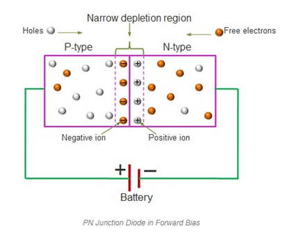
The result of this in a characteristic curve of zero current flowing up to built-in potential is called as “knee current” on the static curves and then a high current flow through the diode with a slight increase in the external voltage as shown below :-
V-I characteristics of PN junction diode in forwarding bias:
The VI characteristics of PN junction diode in forwarding bias are non linear, that is, not a straight line. This non linear characteristic illustrate that during operation of the PN junction, the resistance is not constant. The slope of the PN junction diode in forwarding bias show the resistance is very low. When a forward bias is applied to the diode then it causes a low impedance path and permits to conduct a large amount of current know as “infinite current”. This current start to flow above the knee point with a small amount of external potential.
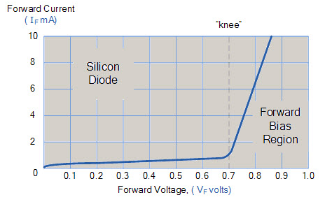
The potential difference across the PN junction is maintained constant by the depletion layer action. The max amount of current to be conducted is kept by the load resistor because when the PN junction diode conducts more current than the normal specifications o the diode, the extra current result in the heat dissipation and leads to serving damage to the device.