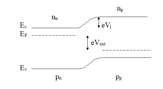
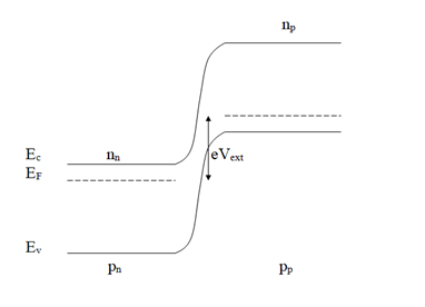
When the external voltage Vext applied. The potential drop across junction is reduced. So np (and pn) increase.
If Vj is the potential drop across the junction.
np/nn = pn/pp = exp(-eVj/kT)
Where we have that
Vj = VB – Vext
Hence,
np/nn = pn/pp = exp(-eVB/kT)exp(eVext/kT) ….. [2]
For zero applied we have that
np0/nn0 = pn0/pp0 = exp(-eVB/kT) …… [1]
We can substitute for exp (-eVB/kT) using eq’ns [1] & [2].
np/nn = np0/nn0 exp(eVext/kT)
pn/pp = pn0/pp0 exp(eVext/kT)
nn is large –plenty of electrons on N-side.
pp is large –plenty of holes on P-side.
They change only slightly when we apply a bias voltage.
i.e. nn » nn0 pp » pp0
So to good approximation we can write
np/np0 = pn/pn0 = exp(eVext/kT)
Can now recall argument used for metal-semiconductor junction – i.e. treat both halves of pn junction as 2 thermionic emitters facing each other.
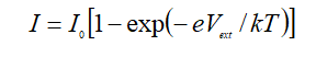
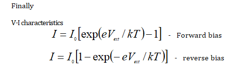
Reverse bias diode:-
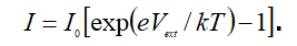
When a PN junction diode is connected in a reverse bias condition, a positive voltage is connected to the N-type and negative voltage is connected to the P-type material.
When the positive voltage is applied to the N-type, then it attracts the electrons near the positive electrode and goes away from the junction, whereas the holes in the P-type end are also attracted away from the junction near the negative electrode.
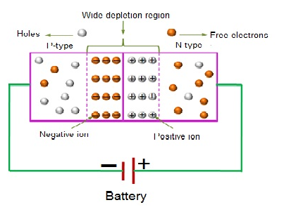
In this type of biasing current flow through the PN junction diode is zero. Though, the current leakage due to minority charge carriers flows in the diode that can be measured in µA. As the potential of the reverse boas to the PN junction diode ultimately increase and leads to PN junction reverse voltage breakdown and the current of the PN junction diode id controlled by an external circuit. Reverse breakdown depends on the doping level of the P *N junction region. Further, with the increase in reverse bias, the diode will become short- circuited due to overheating in the circuit and max current flow in the PN junction diode.
V-I characteristics of PN junction diode in reverse bias:
In this type of bias, the characteristics curve of the diode is shown the fourth quadrant of the below. The current in this biasing is low till breakdown is reached and hence the diode looks like an open circuit. When the input voltage of the reverse bias reached the breakdown voltage, reverse current increase enormously.
Recall Band diagram of reverse biased diode:
In this case the potential drop is across the junction is increase.
So np (and pn) decrease.
Can use similar argument to show that in reverse bias:
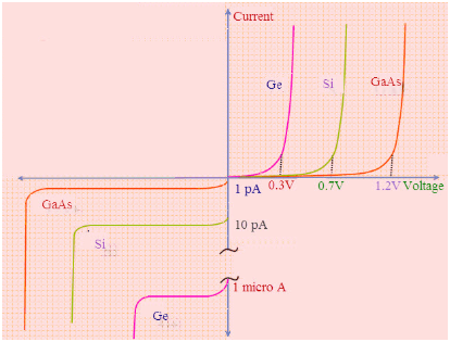
Comparison with Ge, Si and GaAs