After the atomic-power accident in Fukushima, utilization of solar energy has drawn renewed attention from society.1) One of the promising methods to capture solar energy is photovoltaic (solar) cells. Though there are several types of the cells, a present mainstream technology uses semiconductor junctions based on silicon element.2) Silicon is an atom in the fourth group in the periodic table and has four electrons in valence shell. A valence electron orbits the nucleus and stays in the valence shell at low temperature. However, the electron jumps the energy gap (1.12 eV in silicon) into the conduction band if a photon (sunlight) which has greater energy than the gap strikes the electron, and it gets free in the conduction band. On another front, it also leaves behind an electron hole that can move like a physically charged particle (positive). Figure 1(a) shows a schematic diagram of the electron-hole pair generation from the viewpoint of energy band for electron. These electron and hole are called carriers which have the elementary charge (1:602 1019 coulombs) with different sign, and
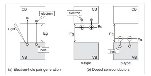
(a) Electron-hole pair generation by sunlight. An electron in the valence band absorbs the energy of light (photons) and jumps the energy gap (1.12 eV in silicon) into the conduction band leaving behind an electron hole (hole). Both electron and hole can move carrying the elementary charge with different sign. (b) Doped semiconductors. Left: An element of 5 valence electrons doped into silicon has the impurity energy level below a conduction band. An extra electron jumps into the conduction band and gets free. The element is positively ionized and called donor. Right: An element of 3 valence electrons doped into silicon has the impurity energy level above a valence band. An electron in the valence band moves to the element leaving a hole. The element is negatively ionized and called acceptor. CB: conduction band, VB: valence band, Eg: energy gap (1.12 eV in silicon), Ea: acceptor impurity level, Ed: donor impurity level)
both contribute a current flow.3) Therefore, it becomes understandable that why the X-ray radiation produces a serious malfunction or damage to the cardiac pacemakers given the fact that it may generate unexpected amount of current at unintended locations in the circuit. Since intrinsic silicon has less ability to conduct electricity, small numbers of different element are doped to the silicon to increase current carriers (electron or hole).
(1) An element with 5 valence electrons such as phosphorous or arsenic is added, which results in one free electron for current conduction. Such impurity element is called a donor (n-type doping).
(2) An element with 3 valence electrons such as gallium or boron is added, which results in one hole for current conduction. Such impurity element is called an acceptor (p-type doping). The former is n-type semiconductor and the latter p-type. A p-n junction diode is formed by placing p-type and n-type semiconductors next to one another.
(3) below schematic diagram of the p-n junction diode and the barrier potential (built-in potential) across the junction. Free electrons near the interface tend to diffuse into the p-type side while free holes near the interface diffuse into the n-type region. A narrow region in the vicinity of the junction which has been depleted of electrons and holes is called the depletion layer. Positive fixed ions (donor ions) are built up on the n-type side of the depletion layer while negative fixed ions (acceptor ions) on the p-type side of the layer. These ions form an electric double layer across the junction. An electric filed from n- to p-type region is created in
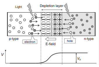
After joining p-type and n-type semiconductors, free electrons near the junction tend to diffuse from n- to p-type region leaving fixed ions with positive charge (donors) in the n-type region while holes near the junction from p- to n-type region leaving fixed ions with negative charge (acceptors). A narrow region in the vicinity of the junction is depleted of free carries, forming the depletion layer. The electric field created by those ions inhibits further diffusion process for both electrons and holes, establishing equilibrium and a built-in potential across the junction. Photons (sunlight) generates electrons and holes that move freely in the region, and the internal electric field in the depletion layer separates electrons from holes. More electrons gather on the n-type and holes on the p-type. This is a driving force to flow a current.
the layer which inhibits any further diffusion of both electrons and holes, and the junction reaches a state of equilibrium. When photons (sunlight) hit the solar cell (p-n junction semiconductor), they are absorbed into the semiconductor and the absorbed energy generates free electrons and holes. The electrons generated in the p-type region within a diffusion length from the interface reach the depletion layer and move into the n-type region while the holes in the n-type region within the diffusion length from the interface similarly move into the p-type region. The internal electric field in the depletion layer separates electrons from holes. The electrons are thus gathered on the n-type side while the holes on the p-type side. This causes more negative in the n-type region and more positive in the p-type. Because of this accumulation of carriers, a current will start to flow when the load is connected to the electrodes placed on both sides. This is the working principle of solar cells
At this equilibrium state, a built-in voltage (Vb) appears across the junction and is described as
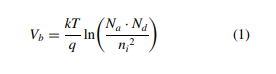
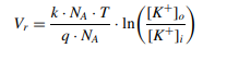
where k is the Boltzmann constant, T the absolute temperature, q the elementary charge, Na and Nd are the concentrations of acceptor and donor atoms, and ni is the carrier concentration of an intrinsic semiconductor (undoped semiconductor). A highly similar equation is featured in a textbook of basic physiology — the membrane resting potential .This is called Goldman Hodgkin-Katz voltage equation and written by
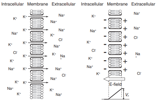
Left: Potassium ions penetrate the membrane from intracellular to extracellular region because the permeability of other ions is much smaller than that of potassium ion in the resting state. Right: Electric double layer is formed across the membrane by potassium ions. The electric field inhibits further penetration and builds up the resting potential.
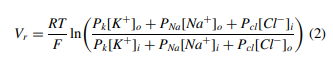
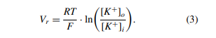
For three major ions , where R is the universal gas constant, T the absolute temperature, F the Faraday constant [ A]0 and [ A]i are the extra- and intracellular concentration of A ion and PA stands for the relative permeability of the ions type A. In most animals cells, the contribution of sodium and chloride ions to the resting potential is negligible compared with potassium ion ( K+) is much higher the resting state than the permeability of sodium (Na+) or ( Cl–) ion. The potassium ions penetrate from intra to extracellular region to form an electric double layer which is similar to across the PN semiconductor junction. The generate electric field across the membrane inhibits any further penetration and build an equilibrium state.
Since the universal gas constant R is represented by R = k x NA and the Faraday constant by F= q x NA (NA: Avogadro constant), the above equation is rewritten by
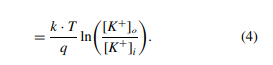
This equation consists of the Boltzmann constant k, the absolute temperature T, the elementary charge q and the natural logarithm of the balance of ions and closely resembles the barrier potential Vb across the p-n junction in a semiconductor diode (see eq. (1)). Although it is hardly surprising that the natural phenomena caused by the subatomic particles and/or atomic ions resemble because such phenomena are usually described using the universal constants, it is still very interesting that a physical quantity (potential) in the apparently different materials such as a cell membrane and a semiconductor can be described in a similar manner.